摘要:本文主要从 Sn‐Ag‐Cu 无铅钎料的熔化温度、润湿铺展性、界面显微组织以及焊点可靠性这四个方面出发,结合国内外研究现状,综述了添加微量元素以及纳米颗粒对 Sn‐Ag‐Cu 无铅钎料组织和性能的影响,并且综合分析了它们的影响机理。
0 前言
在传统电子封装工艺中,Sn‐Pb 系钎料(共晶温度约为 183℃左右)凭借其优良的综合性能以及 低廉的生产成本等优势受到广泛应用。但考虑到 Pb 对人体以及环境的危害,在国际立法的推动下, 电子工业开始实行无铅化发展。目前具有应用、发展潜力的钎料体系主要有 Sn‐Ag,Sn‐Bi,Sn‐Cu 等。
二元系无铅钎料,以及在此基础上衍生出来的 Sn‐Ag‐Cu,Sn‐Ag‐Bi,Sn‐Cu‐Ni,Sn‐Zn‐Bi 等三元系无铅 钎料[1]。其中,Sn‐Ag‐Cu 三元系无铅钎料因其力学性能优越、润湿性能好等原因成为传统 Sn‐Pb 系钎 料的最佳替代品。然而,与传统 Sn‐Pb 系钎料相比,Sn‐Ag‐Cu 系无铅钎料仍存在许多不足,例如抗 氧化能力较弱、熔点较高、钎料与基板界面处金属间化合物(Intermetallic compound, IMC)过量生 长以及生产成本较高等。近年来,诸多研究表明,Sn‐Ag‐Cu 系无铅钎料的上述不足可以通过微量元 素合金化的方法得到弥补[2,3]。与此同时,具有尺寸小、比表面积大、表面能高、表面原子所占比例 大等特点的纳米颗粒也开始倍受科研工作者的关注。他们通过试验发现,在 Sn‐Ag‐Cu 无铅钎料中添 加适量的纳米颗粒不仅能细化钎料的显微组织而且又可以显著提高焊点的可靠性[4]。本文主要从 Sn‐Ag‐Cu 无铅钎料的熔化温度、润湿铺展性、界面显微组织以及焊点可靠性这四个方面出发,结合 国内外研究现状,综述了添加微量元素以及纳米颗粒对 Sn‐Ag‐Cu 无铅钎料组织和性能的影响,并综 合分析了它们的影响机理。
1 钎料的熔化温度
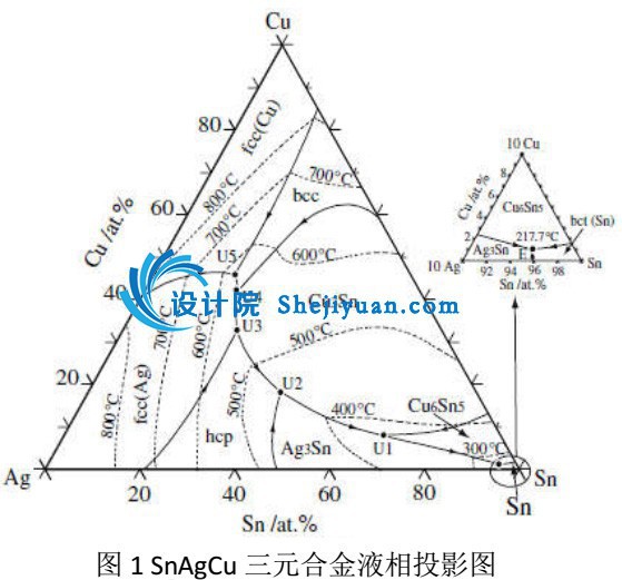
若要替代传统的 Sn‐Pb 钎料,研制的新型钎料的熔化温度应与其相近,这样便可以沿袭原有的 焊接工艺和设备,节约生产成本。此外,若熔点过高会使母材晶粒长大、过烧或局部熔化,最终导 致焊点的可靠性大幅下降。由图 1 所示的 SnAgCu 三元合金相图[5]可知,SnAgCu 三元合金的共晶温度 约为 217℃,与传统 Sn‐37Pb 共晶钎料(共晶温度约为 183℃)相比,其熔点提高了近 18.6%[6]。因 此,降低钎料熔点的工作亟需进行。
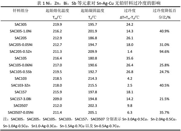
目前研究者们多采用微量元素合金化的方法来降低钎料熔点。其中,元素 Ga 和 Bi 因其具有相 对较低的熔点,在 Sn‐Ag‐Cu 钎料中添加后都能在一定程度上降低钎料的熔点。此外,适量添加 Bi 还可以在一定程度上减小 Sn‐1.5Ag‐0.7Cu 的过冷度,使得钎料冷却时所需的结晶驱动力下降,提高 了钎焊效率,节约了生产成本[7,8]。此外,适量添加 Ni,Zn,Bi,Sb 等元素也均能在一定程度上降低 Sn‐Ag‐Cu 无铅钎料过冷度,具体如表 1 所示。其中,Zn 的降低效果最为显著,添加 0.5wt.% Zn 的 Sn‐2.0Ag‐0.5Cu 的过冷度相对于未添加前降低了94.6%。同时,通过比较Sn‐3.0Ag‐0.5Cu,Sn‐2.0Ag‐0.5Cu以及 Sn‐1.0Ag‐0.5Cu 的过冷度可以发现:随着 Ag 含量的降低,钎料所需过冷度反而增加。因此,若 要推进低银 Sn‐Ag‐Cu 无铅钎料的发展,钎料过冷度的问题也亟需解决[9‐12]。此外,随着纳米颗粒添 加的兴起,大部分研究者却发现诸如 SiC[13],TiO2[14],ZrO2[15]等纳米颗粒以及石墨烯纳米片[16]均不能 显著降低 Sn‐Ag‐Cu 无铅钎料的熔点。
2 钎料的润湿性能
在钎焊的初始阶段,熔融的钎料会在基板上润湿铺展,平衡状态时钎料与基板间形成的润湿角
θ 由界面张力决定,两者的关系可用杨氏方程cos ( sg sl ) / 1 g 表示(其中 σsg 为固体表面张力,
σlg 为液体表面张力,σsl 为液固界面张力)。由该方程可知,液体表面张力 σlg 越小,润湿角 θ 也就越 小,润湿性能也就越好。良好的润湿性能是新型无铅钎料形成可靠焊点的必要前提之一[1,17]。
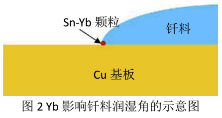
目前,研究者们发现无论是微量元素合金化还是适量添加纳米颗粒都是通过减小熔融钎料表面 张力的方法来改善润湿性能的。有关研究结果如下:一定条件下,当 In[18]在 Sn‐1.2Ag‐0.5Cu 中的添 加量为 0.4wt%——0.6wt%时,Ga[19]在 Sn‐0.3Ag‐0.7Cu 中的添加量为 0.5wt%时,Zn[20]在 Sn‐Ag‐Cu 中的添加量为 0.8wt%时,各自钎料的润湿性能均能显著改善。但若过量,钎料的润湿性能又会大幅下降, 特别是 Zn,其易氧化,当添加量上升到 3wt%时,会在熔融钎料中产生氧化渣,反而阻碍了钎料在 基板上的润湿。试验发现,当在 Sn‐Ag‐Cu 无铅钎料中分别添加稀土元素 Eu[21]或 Yb[22],并且添加量 达 0.05wt%时,Sn‐Ag‐Cu 无铅钎料的润湿性能均得到显著改善。其中,Yb 是亲 Sn 元素,会与 Sn 形 成 Sn‐Yb 颗粒,若此颗粒存在于熔融此时钎料的润湿钎料、Cu 基板以及空气的三角点处时(如图 2 所示),熔融钎料的表面张力将会下降,因此润湿性能得到提升。但若 Yb 的含量过高,由 Yb 形成的 稀土氧化物会明显减弱钎料的润湿能力。此外,有研究表明,在无铅钎料中适量添加 Al2O3[23], BaTiO3[24],Fe2O3[25],TiO2[26]等纳米颗粒以及 SiC 纳米晶须[27]也均能通过降低熔融钎料的表面张力从 而达到改善无铅钎料润湿性能的目的。
3 界面显微组织
在钎焊过程中,当熔融的钎料在基板上润湿铺展时,会在界面处形成金属间化合物即 IMC。随 着时间的增长,IMC 长大并且会逐渐成层状分布在界面处。由于 IMC 较脆,若界面处 IMC 层过厚, 会使焊点在服役过程中的力学性能下降,焊点可靠性变差[1]。
近些年,科研工作者大都通过适量添加微量元素或纳米颗粒的方式来降低 Sn‐Ag‐Cu 无铅钎料与 基板界面处 IMC 厚度,其作用原理大致可以分为:(1)添加的元素如 Al[28],Ga[7,29]或 Ni 纳米颗粒[30] 等能够与 Cu 或 Sn 原子在界面处形成新的界面层,阻碍 Cu 或 Sn 原子的扩散。例如 Al 能够在 Sn‐3.8Ag‐0.7Cu/Cu 基板界面处生成含 Al 的界面层,该界面层可以阻碍 Sn 原子扩散,抑制了界面处 Cu6Sn5 的生长,从而降低了界面层厚度;Ga 元素能与 Cu 基板之间会形成 Cu2Ga 界面层,在时效过 程中它能作为扩散的阻碍层抑制其它界面层的生长。当 Ga 在 Sn‐0.5Ag‐0.7Cu 钎料中的添加量为 0.5wt%时,界面层厚度相对于原始钎料降低了约 58.9%(2)添加的元素如 Zn[31],In[32]等能替代部分
Cu6Sn5 或 Cu3Sn 中的Cu 或Sn 原子,改变 Cu 或 Sn 原子的扩散途径。例如 Zn 原子会替代 Sn‐3.5Ag‐1.0Cu
无铅钎料/Cu 界面处 Cu6Sn5 中的 Cu 原子,形成(Cu,Zn)6Sn5,减少界面层和 Cu 基板间扩散通道的数量, 从而抑制了界面层的生长。当 Zn 的含量为 0.4wt%时,其抑制效果达到最佳。(3)添加的如 Pr[33], Nd[34],La[35]等大部分稀土元素具有亲 Sn 性,降低了 Sn 原子的活度,减少了界面层 Cu6Sn5 的形成。 此外,钎料中形成的 PrSn3,Nd‐Sn 颗粒等可以作为熔融钎料中的形核质点,加速钎料的凝固过程, 使得 IMC 没有充分的时间生长。(4)在钎焊过程中,添加的纳米颗粒如 Mn[36],Mo[37],Y2O3[38]等既 不熔化,也不与界面处其他原子结合,只吸附在 Cu6Sn5 的表面,通过抑制 Cu 或 Sn 原子的扩散来降 低界面层的厚度。例如 Mn 纳米颗粒的熔点约为 1246℃,在 250℃的回流温度下不能熔化,在扇贝 状的 Cu6Sn5 表面吸附,阻碍 Cu 基板中的 Cu 原子向熔融钎料中扩散,使得 Sn‐3.8Ag‐0.7Cu/Cu 的界面 层厚度下降。
4 焊点可靠性
随着电子元器件逐渐向小尺寸化、多功能化方向的转变,无疑也给在电子器件中起到机械支撑 和电气连接作用的微焊点提出更为苛刻的要求。微焊点在服役期间承受交变温度场的作用,会因产 生的热应力而发生疲劳破坏,最终导致电子产品提前失效。目前,焊点可靠性评估主要集中在热循 环、高温时效以及冲击等方面[39]。
焊点可靠性的提高得益于:(1)添加的微量元素如 Zn[19],La[40]等对基体或界面处晶粒的细化。 例如在 Sn‐Ag‐Cu 无铅钎料中添加 0.8wt%的 Zn 可以使枝状的 β‐Sn 逐渐转变为晶粒状,同时,形成的Cu‐Zn 颗粒会均匀分布在钎料基体中,使得焊点在‐55℃‐125℃之间的温度循环测试下的抗热疲劳性 也相应地提高。(2)添加的微量元素如 Al[41],Pd[42]或如 TiO2[43],Co[44]等纳米颗粒对钎料基体中或界 面处 IMC 生长的抑制。例如在 Sn‐1.0Ag‐0.5Cu 添加 0.1wt%的 Al 能抑制界面处 Cu6Sn5 的生长,时效过 后,界面层厚度下降,焊点可靠性提高;当 Sn‐3Ag‐0.5Cu 钎料中 Pd 含量低于 0.2wt%时,由于界面 处形成(Cu,Ni)6Sn5 界面层呈连续状,因此钎料的可靠性上升;当 Pd 含量达到 0.3wt%时,出现了新增 相(Pd,Ni)Sn4,使焊点抗高速推球剪切的能力下降,焊点的机械可靠性也随之下降。(3)添加的微量 元素如 Eu[21],Yb[22]等所形成的如 EuSn3,Sn‐Yb 沉淀颗粒对蠕变变形过程中位错运动的阻碍。具体说 来,由于 Eu 的亲 Sn 性,使得 Cu‐Sn 以及 Ag‐Sn 的反应动力下降,细化了 Cu6Sn5 和 Ag3Sn 颗粒,它们 和 EuSn3 会在熔融的钎料中沉淀下来,最终能阻碍蠕变过程中位错的移动,提高了钎料的抗蠕变性。 当 Eu 在 Sn‐Ag‐Cu 无铅钎料中的添加量达 0.04wt%时,钎料的抗蠕变寿命是未添加 Eu 时的 8.5 倍, 抗热疲劳寿命提高了 37.4%。
5 结论
为了满足电子封装行业无铅化、低成本以及高可靠性的发展需求,Sn‐Ag‐Cu 无铅钎料将是今后 很长一段时间内的发展重点。在 Sn‐Ag‐Cu 无铅钎料中添加微量元素或纳米颗粒,对降低钎料熔点, 改善润湿铺展性能,减小界面层厚度,增强焊点可靠性方面均起到了一定程度的积极作用。但是添 加时应遵循适量的原则,否则反而会恶化 Sn‐Ag‐Cu 无铅钎料这些方面的性能。
参考文献:
[1]陈建勋, 赵兴科, 刘大勇, 黄继华, 邹旭晨. 电子组装用 SnAgCu 系无铅钎料的研究进展[J]. 材料工程, 2013, 09: 91‐98.
[2]Sun L, Zhang L. Properties and Microstructures of Sn‐Ag‐Cu‐X Lead‐Free Solder Joints in Electronic Packaging[J]. Advances in Materials Science and Engineering, 2015, 2015.
[3]Gao L, Xue S, Zhang L, et al. Effect of alloying elements on properties and microstructures of SnAgCu solders[J]. Microelectronic Engineering, 2010, 87(11): 2025‐2034.
[4]马运柱, 李永君, 刘文胜. 纳米颗粒增强无铅复合焊料的研究现状[J]. 电子元件与材料, 2011, 30(06): 79‐83.
[5]Liu X J, Wang C P, Gao F, et al. Thermodynamic Calculation of Phase Equilibria in the Sn‐Ag‐Cu‐Ni‐Au System[J]. Journal of Electronic Materials. 2007, 36(11): 1429‐1441.
[6]El‐Daly A A, Hammad A E, Al‐Ganainy G S, et al. Properties enhancement of low Ag‐content Sn‐Ag‐Cu lead‐free solders containing small amount of Zn[J]. Journal of Alloys and Compounds. 2014, 614: 20‐28.
[7]Luo D, Xue S, Liu S. Investigation on the intermetallic compound layer growth of Sn‐0.5Ag‐0.7Cu‐xGa/Cu solder joints during isothermal aging[J]. Journal of Materials Science: Materials in Electronics, 2014, 25(12): 5195‐5200.
[8]El‐Daly A A, El‐Taher A M, Gouda S. Novel Bi‐containing Sn‐1.5Ag‐0.7Cu lead‐free solder alloy with further enhanced thermal property and strength for mobile products[J]. Materials & Design. 2015, 65: 796‐805.
[9]El‐Daly A A, El‐Taher A M. Evolution of thermal property and creep resistance of Ni and Zn‐doped Sn‐2.0Ag‐0.5Cu lead‐free solders[J]. Materials & Design. 2013, 51: 789‐796.
[10]El‐Daly A A, El‐Taher A M, Dalloul T R. Enhanced ductility and mechanical strength of Ni‐doped Sn‐3.0Ag‐0.5Cu lead‐free solders[J]. Materials & Design. 2014, 55: 309‐318.
[11]Hammad A E. Evolution of microstructure, thermal and creep properties of Ni‐doped Sn‐0.5Ag‐0.7Cu low‐Ag solder alloys for electronic applications[J]. Materials & Design. 2013, 52: 663‐670.
[12]El‐Daly A A, Hammad A E, Fawzy A, et al. Microstructure, mechanical properties, and deformation behavior of Sn‐1.0Ag‐0.5Cu solder after Ni and Sb additions[J]. Materials & Design. 2013, 43: 40‐49.
[13]El‐Daly A A, Fawzy A, Mansour S F, et al. Thermal analysis and mechanical properties of Sn‐1.0Ag‐0.5Cu solder alloy after modification with SiC nano‐sized particles[J]. Journal of Materials Science: Materials in Electronics. 2013, 24(8): 2976‐2988.
[14]Tang Y, Pan Y C, Li G Y. Influence of TiO2 nanoparticles on thermal property, wettability and interfacial reaction in Sn‐3.0Ag‐0.5Cu‐xTiO2 composite solder[J]. Journal of Materials Science: Materials in Electronics. 2013, 24(5):1587‐1594.
[15]Gain A K, Chan Y C. Growth mechanism of intermetallic compounds and damping properties of Sn‐Ag‐Cu‐1wt% nano‐ZrO2 composite solders[J]. Microelectronics Reliability. 2014, 54(5): 945‐955.
[16]Liu X D, Han Y D, Jing H Y, et al. Effect of graphene nanosheets reinforcement on the performance of Sn‐Ag‐Cu lead‐free solder[J]. Materials Science and Engineering: A, 2013, 562: 25‐32.。
[17]张莎莎, 张亦杰, 马乃恒, 王浩伟. Sn‐Ag‐Cu 系无铅焊料性能研究进展[J]. 热加工工艺, 2010, 39(01): 124‐127.
[18]Yu A M, Kim M S, Lee C W, et al. Wetting and interfacial reaction characteristics of Sn‐1.2Ag‐0.5Cu‐xIn quaternary solder alloys[J]. metals and Materials International, 2011, 17(3): 521‐526.
[19]Zhang L, Han J, He C, et al. Effect of Zn on properties and microstructure of SnAgCu alloy[J]. Journal of Materials Science: Materials in Electronics, 2012, 23(11): 1950‐1956.
[20]Luo D, Xue S, Li Z. Effects of Ga addition on microstructure and properties of Sn–0.5 Ag–0.7 Cu solder[J]. Journal of Materials Science: Materials in Electronics, 2014, 25(8): 3566‐3571.
[21]Zhang L, Han J, Guo Y, et al. Properties and microstructures of SnAgCu‐xEu alloys for concentrator silicon solar cells solder layer[J]. Solar Energy Materials and Solar Cells, 2014, 130: 397‐400.
[22]Zhang L, Fan X, Guo Y, et al. Properties enhancement of SnAgCu solders containing rare earth Yb[J]. Materials & Design, 2014, 57: 646‐651.
[23]Huang B, Chen G, Wu F, et al. Preparation, microstructure and properties of Sn‐Ag‐Cu solder reinforced with Al2O3 nanoparticles[C]//Electronic Packaging Technology (ICEPT), 2014 15th International Conference on. IEEE, 2014: 243‐246.
[24]Yang L, Ge J, Zhang Y, et al. Effect of BaTiO3 on the microstructure and mechanical properties of Sn1.0Ag0.5Cu lead‐free solder[J]. Journal of Materials Science: Materials in Electronics. 2015, 26(1): 613‐619.
[25]Gu Y, Zhao X, Li Y, et al. Effect of nano‐Fe2O3 additions on wettability and interfacial intermetallic growth of low‐Ag content Sn‐Ag‐Cu solders on Cu substrates[J]. Journal of Alloys and Compounds. 2015, 627: 39‐47.
[26]Li Y, Zhao X, Liu Y, et al. Effect of TiO2 addition concentration on the wettability and intermetallic compounds growth of Sn3.0Ag0.5Cu‐xTiO2 nano‐composite solders[J]. Journal of Materials Science: Materials in Electronics. 2014, 25(9): 3816‐3827.
[27]Xu K, Chen G, Wu F, et al. Effect of SiC whiskers addition on microstructure, microhardness and wettablility of Sn‐Ag‐Cu solder[C]. Electronic Packaging Technology (ICEPT), 2014 15th International Conference on IEEE. 2014: 310‐312.
[28]Li J F, Agyakwa P A, Johnson C M. Effect of trace Al on growth rates of intermetallic compound layers between Sn‐based solders and Cu substrate[J]. Journal of Alloys and Compounds, 2012, 545: 70‐79.
[29]Zhang Q K, Long W M, Yu X Q, et al. Effects of Ga addition on microstructure and properties of Sn‐Ag‐Cu/Cu solder joints[J]. Journal of Alloys and Compounds. 2015, 622: 973‐978.
[30]Fouzder T, Li Q, Chan Y C, et al. Interfacial microstructure and hardness of nickel (Ni) nanoparticle‐doped tin‐silver‐copper (Sn‐Ag‐Cu) solders on immersion silver (Ag)‐plated copper (Cu) substrates[J]. Journal of Materials Science: Materials in Electronics, 2014, 25(9): 4012‐4023.
[31]Mayappan R, Yahya I, Ab Ghani N A, et al. The effect of adding Zn into the Sn‐Ag‐Cu solder on the intermetallic growth rate[J]. Journal of Materials Science: Materials in Electronics, 2014, 25(7): 2913‐2922.
[32]Lejuste C, Hodaj F, Petit L. Solid state interaction between a Sn‐Ag‐Cu‐In solder alloy and Cu substrate[J]. Intermetallics, 2013, 36: 102‐108.
[33]Gao L, Xue S, Zhang L, et al. Effect of praseodymium on the microstructure and properties of Sn3.8Ag0.7Cu solder[J]. Journal of Materials Science: Materials in Electronics, 2010, 21(9): 910‐916.
[34]Gao L, Xue S, Zhang L, et al. Effects of trace rare earth Nd addition on microstructure and properties of SnAgCu solder[J]. Journal of Materials Science: Materials in Electronics, 2010, 21(7): 643‐648.
[35]王佳, 王丽凤, 刘学. La 对 SnAgCu/Cu 及 Ni 界面金属间化合物的影响[J]. 电子元件与材料, 2011, 30(5): 68‐71.
[36]Xiang K K, Haseeb A, Arafat M M, et al. Effects of Mn nanoparticles on wettability and intermetallic compounds inbetween Sn‐3.8Ag‐0.7Cu and Cu substrate during multiple reflow[C]. Quality Electronic Design (ASQED), 2012 4th Asia
Symposium on IEEE. 2012: 297‐301.
[37]Haseeb A, Arafat M M, Johan M R. Stability of molybdenum nanoparticles in Sn‐3.8Ag‐0.7Cu solder during multiple reflow and their influence on interfacial intermetallic compounds[J]. Materials Characterization, 2012, 64: 27‐35.
[38]Yang L M, Zhang Z F. Effects of Y2O3 Nanoparticles on Growth Behaviors of Cu6Sn5 Grains in Soldering Reaction[J]. Journal of electronic materials, 2013, 42(12): 3552‐3558.
[39]张亮. SnAgCu 系无铅焊点可靠性及相关理论研究[D]. 南京: 南京航空航天大学, 2011.
[40]Sadiq M, Pesci R, Cherkaoui M. Impact of thermal aging on the microstructure evolution and mechanical properties of lanthanum‐doped Tin‐Silver‐Copper lead‐free solders[J]. Journal of electronic materials, 2013, 42(3): 492‐501.
[41]Sabri M F M, Shnawah D A, Badruddin I A, et al. Effects of aging on Sn‐1Ag‐0.5 Cu solder alloys containing 0.1 wt.% and 0.5 wt.% Al[J]. Journal of Alloys and Compounds, 2014, 582: 437‐446.
[42]Ho C E, Hsu L H, Lin S W, et al. Influence of Pd Concentration on the Interfacial Reaction and Mechanical Reliability of the Ni/Sn‐Ag‐Cu‐xPd System[J]. Journal of electronic materials, 2012, 41(1): 2‐10.
[43]Tsao L C, Huang W T, Wu M W, et al. Suppressing effect of 1 wt.% nano‐TiO2 addition into low Ag content Sn‐Ag‐Cu solder alloy on the intermetallic growth with Cu substrate during isothermal aging[C]//Electronic Packaging Technology and High Density Packaging (ICEPT‐HDP), 2012 13th International Conference on. IEEE, 2012: 465‐468.
[44]Haseeb A, Leng T S. Effects of Co nanoparticle addition to Sn‐3.8Ag‐0.7Cu solder on interfacial structure after reflow and ageing[J]. Intermetallics, 2011, 19(5): 707‐712.


